Here in this tutorial section you will be all gaining information about how these ic works and how you are gonna use them.
Some of the most famous ic’s for this purpose are :-
- Adc0808
- Adc0804
Adc0804
ADC0804 is a very commonly used 8-bit analog to digital convertor. It is a single channel IC, i.e., it can take only one analog signal as input.It has no multiplexed input capability like 0808. The digital outputs vary from 0 to a maximum of 255. The step size can be adjusted by setting the reference voltage at pin9. When this pin is not connected, the default reference voltage is the operating voltage, i.e., Vcc.Step size at 5V is 19.53mV (5V/255), i.e., for every 19.53mV rise in the analog input, the output varies by 1 unit. To set a particular voltage level as the reference value, this pin is connected to half the voltage. For example, to set a reference of 4V (Vref), pin9 is connected to 2V (Vref/2), thereby reducing the step size to 15.62mV (4V/255).
ADC0804 needs a clock to operate. The time taken to convert the analog value to digital value is dependent on this clock source. An external clock can be given at the Clock IN pin. ADC 0804 also has an inbuilt clock which can be used in absence of external clock. A suitable RC circuit is connected between the Clock IN and Clock R pins to use the internal clock.
Pin no. Function
1 Activates ADC; Active low
2 Input pin; High to low pulse brings the data from internal registers to the output pins after conversion
3 Input pin; Low to high pulse is given to start the conversion
4 Clock Input pin; to give external clock.
5 Output pin; Goes low when conversion is complete
6 Analog non-inverting input
7 Analog inverting Input; normally ground
8 Ground(0V)
9 Input pin; sets the reference voltage for analog input
10 Ground(0V)
11-18 8 bit digital output pins
19 Used with Clock IN pin when internal clock source is used
20 Supply voltage; 5V
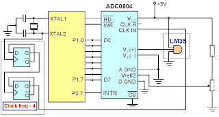
8-bit digital data is D0-D7 is read in a port of 8-bit microcontroller.Analog value is read from Vin(+)(here LM35 is shown in figure).
In MCU make function as :-
ReadADC( )
{
while(INTR is high)
{ wait }
Set Read pin to high ;
Read port in integer variable;
Set READ pin to low;
}
But make it sure that rest of your procedure finishes within clock freq/4 time or else either use more flip flops to divide clock frequencies or u can do it by further modification in code..
Think it. how will you make it through code…. J
ADC0808
The ADC0808, ADC0809 data acquisition component is a monolithic CMOS device with an 8-bit analog-to-digital converter, 8-channel multiplexer and microprocessor compatible control logic. The 8-bit A/D converter uses successive approximation
as the conversion technique. The converter features a high impedance chopper stabilized comparator, a 256R voltage divider with analog switch tree and a successive
approximation register. The 8-channel multiplexer can directly access any of 8-single-ended analog signals. The device eliminates the need for external zero and full-scale
adjustments. Easy interfacing to microprocessors is provided by the latched and decoded multiplexer address inputs and latched TTL TRI-STATE outputs.
Features
■ Easy interface to all microprocessors
■ Operates ratiometrically or with 5 VDC or analog span
adjusted voltage reference
■ No zero or full-scale adjust required
■ 8-channel multiplexer with address logic
■ 0V to VCC input range
■ Outputs meet TTL voltage level specifications
■ ADC0808 equivalent to MM74C949
■ ADC0809 equivalent to MM74C949-1
Key Specifications
■ Resolution 8 Bits
■ Total Unadjusted Error ±½ LSB and ±1 LSB
■ Single Supply 5 VDC
■ Low Power 15 mW
■ Conversion Time 100 μs

